Food Grade plastic Bag for bread packing. About the size, their width, length and thickness could be just as you order. For the color, they could in clear or other colors as you require. The bags could also be on roll or on sheet. With easy opening technique, our bread bags can keep the breads clean and sanitary and suitable been used in bakery, dessert house,cake shops or market.
Reusable Bread Bag,Linen Bread Bag,Paper Bread Bags,Cotton Bread Bag,Loaf Bread Bags,Bread Plastic Bag BILLION PLASTIC MANUFACTURING CO.,LTD, JIANGMEN , https://www.jmtshirtbag.com
introduction
The storage test technique [1] method is an effective method of recording the parameters of a moving object in a special environment. It stores the test data in memory first, and after the device is recovered, it communicates with the host computer through a specific interface and restores the data information. In many consumer electronics products, higher requirements are placed on the real-time performance and power consumption of data acquisition and storage systems. Not only must low-power and miniaturized designs be met at the same time, but also real-time changes in the data collected in the field. In this way, higher sampling rates, power consumption, etc. must be put forward for the system. With the development of semiconductor technology, advances in various technologies have enabled high-speed, low-power data acquisition systems to be implemented.
This article mainly uses Philips 16/32-bit microcontroller LPC2148 [2  3] as the core control element, through the use of nRF24L01 [4] combined to achieve data acquisition, storage and transmission.
1 System principle
The entire test system consists of an analog adaptation circuit, an external crystal oscillator, a microcontroller, a memory module, a power management module, a wireless transceiver module, and an interface circuit, as shown in FIG. 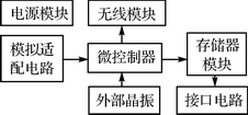
Figure 1 System Block Diagram
The design of the power supply module is the core part of saving the entire system. That is, the power supply only needs to be supplied to each circuit module when it is needed. When it is not needed, it can be powered off to reduce the invalid power consumption of the system. Single-battery power supply can be used to implement multi-branch power network management, making the power of each module of the system relatively independent. However, at this time, it is necessary to pay attention to compatibility issues between live parts and uncharge parts.
1.2 Analog Adapter Circuit
Since the signal measured by the sensor is very weak, it is necessary to perform a series of processing after appropriate amplification and filtering.
1.3 Microcontrollers
The test system selected Philips 16/32-bit microcontroller LPC2148 as the core control element. It comes with its own 10-bit A/D converter, which eliminates the need for an external A/D converter, which means it can be smaller and save costs. At the same time it also has power-saving mode and idle mode power saving mode, rational design can reduce system power consumption.
1.4 Interface Circuit and Wireless Transceiver Section
The test system has two methods to communicate with the host computer, one is implemented through the wireless transceiver module nRF24L01, and the other is implemented through a specific interface circuit, so that even if there is an error in the wireless transmission part, it can ensure that the data is recovered afterwards.
2 Introduction to the hardware and software of the main part of the system
2.1 Development of Internal A/D Converter
The LPC2148 has two 10-bit successive approximation analog-to-digital converters. The eight pins are multiplexed as input pins (ADC0 and ADC1). It has a power-down mode and the measurement range is 0 V~VREF. The conversion time of 10 bits is ≥ 2.44 μs, burst conversion mode with one or more inputs, optionally triggered by an input transition or a timer match signal. Its basic clock is provided by the VPB (VLSI Peripheral Bus) clock, and each converter contains a programmable divider that can adjust the clock to 4.5 MHz (maximum) required for step-by-step conversion. Fully-accurate conversion requirements are required 11 such clocks. This document uses the LPC2148 I/O port to implement voltage measurement using channel 3 of the ADC module, defining I/O port P0.30 as AD0.3, sampling the voltage through the arrival of a timer interrupt, and the ADC register. The settings are as follows:
AD0CR=(1<<3)| //SEL=8, select channel 3
((Fpclk/1000000-1)<<8)| //CLKDIV= Fpclk/1000000-1, the conversion clock is 1 MHz
(0<<16)| //BURST=0, software control conversion operation
(0<<17)| //CLKS=0, use 11clock conversion
(1<<21)| //PDN=1, normal operation mode
(0<<22)| //TEST1:0=00, normal operation mode
(1<<24)| //START=1, start A/D conversion directly
(0<<27)| // This bit is invalid when directly starting A/D conversion
DelayNS(10);
ADC_Data=AD0DR;//Read the A/D conversion result and clear the DONE flag
While(1){
AD0CR|=1<<24; //Perform the first conversion
While((AD0STAT&0x80000000)==0);//wait for conversion to end
AD0CR|=1<<24; //Start the conversion again
While((AD0STAT&0x80000000)==0);//wait for conversion to end
ADC_Data=AD0DR;//Read A/D conversion result
}
2.2 Communication between SPI and nRF24L01 Modules
SPI is a full-duplex serial interface. It is designed to handle multiple interconnected masters and slaves on a given bus. Only one host and one slave can communicate on the interface during a given data transfer. During a data transfer, the master always sends 8 to 16 bits of data to the slave, and the slave always sends one byte of data to the master. Figure 2 shows the timing of the transmission format for the four different SPI data. 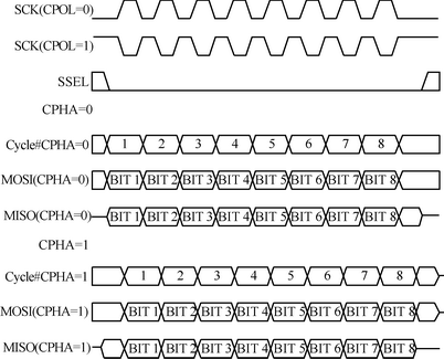
Figure 2 SPI data transmission format
The part of the SPI initialization code is as follows:
Void MSIP_Init(void){
PINSEL0=(PINSEL0&(~(0xff<<8)))|(0x55<<8); // Set pin connection SPI
SPCCR = 0x52; / / set the SPI clock divider
SPCR=(0<<3)| //CPHA=0, data is sampled on the first clock edge of SCK
(1<<4)| //CPOL=1, SCK is active low
(1<<5)| //MSTR=1, SPI is in master mode
(0<<6)| //LSBF=0, SPI data transmission MSB (bit 7) first
(0<<7); //SPIE=0, SPI interrupt is disabled
} 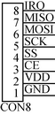
Figure 3 interface circuit
These 8 pins are respectively connected with the GPIO port of the microcontroller, and the microcontroller is set to corresponding functions when it is initialized. GND is the power ground; VDD is the positive power supply 1.9~3.6 V output; CE is the operating mode selection, RX or TX mode; SS is the SPI chip select enable, low level enable; SCK is the SPI clock; MOSI is the SPI input MISO is SPI output; IRQ is interrupt output.
The receiver part of the code is as follows:
#Include "NRF24L01.h"
Unsigned int RxBuf[5]; // Receive buffer, save received data
Int main(){
NRF24L01_Initial(); //nRF24L01 initialization
While((NRF24L01_RxStatus())!=1){//nRF24L01 has no data request
*P_Watchdog_Clear=0x0001;
}
NRF24L01_ReceiveByte(RxBuf);//Receive data
While(1){
*P_Watchdog_Clear=0x0001;
}
}
3 Experimental data and verification
Figure 4 shows two experimental curves measured with this test system. This curve measures the amount of voltage in the fuze battery [8]. The curve can be divided into two parts, one part is that the battery voltage increases with time, and the other part is that the voltage amount remains unchanged with time. This is due to the special structure of the fuse.
After experimental demonstration, the test system can meet the measurement accuracy requirements within the allowable error range, thus verifying the test system has a strong application.
4 Outlook
The future embedded products are hardware and software devices that are tightly integrated. In order to reduce power consumption and costs, designers need to simplify the system kernel as much as possible, and only retain hardware and software that are closely related to system functions, and use the lowest resources to achieve the most appropriate functions. All have low power consumption, small size, high degree of integration [9]. Embedded systems and specific applications are organically combined. Its upgrading is also synchronized with specific products. Therefore, once embedded system products enter the market, they have a long life cycle and huge market potential. 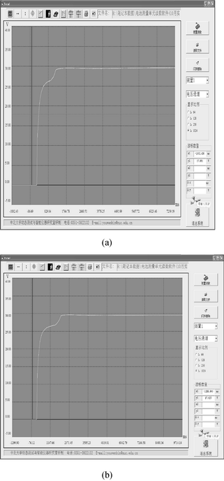
Figure 4 Experiment curve
[1] Zu Jing, Shen Xiangnan, Zhang Wendong. Storage Testing Technology [J]. Journal of Ordnance, 1995(2).
[2] Zhou Ligong, et al. Easy to understand ARM7——LPC213x/214x[M]. Beijing: Beijing University of Aeronautics and Astronautics Press, 2005.
[3] Zhou Ligong, et al. ARM embedded system basic tutorial [M]. Beijing: Beijing University of Aeronautics and Astronautics Press, 2005.
[4] nRF2401 and SPI Interface [EB/OL].[20080218].http://SPI%20interface.pdf.
[5] ARM Inc. ARM Developer Suite_CodeWarrior IDE Guide, 2000.
[6] ARM Inc. ARM Developer Suite_Compliers and Libraries, 2000.
[7] ARM Inc. ARM Developer Suite_Assembler Guide, 2000.
[8] Wang Yingche, Tian Wei, Zhu Yapeng. Application of lead-acid reserve battery in non-rotating missile fuses[J]. Journal of Detection and Control, 2008,30(5):5256.
[9] http://baike.baidu.com/view/6115.htm?fr=ala0_1_1.
Sun Tingting (Graduate student), Ma Tiehua (professor, doctoral tutor), Shen Dawei (lecturer), the main research direction for dynamic testing and intelligent instruments.
Author: Sun Tingting Ma Tiehua Shambaugh Source: "Microcontroller and Embedded Systems"

Embedded system storage test technology and wireless transmission applications [Figure]
Abstract: Storage testing technology is the most effective method to record the parameters of moving objects in special environments. This article describes how to develop a storage test system based on ARM7 LPC21xx. The Philips 16/32-bit microcontroller LPC21xx is based on a 16/32-bit ARM7TDMI-S CPU-based microcontroller that supports real-time emulation and embedded tracking. It features both power-down and idle power-saving modes, battery-operable and long-term jobs. Use the microcontroller's own internal 10-bit A/D converter to sample and use the SPI to communicate with the nRF24L01 module. 1.1 Power Module In setting the register, note the difference between CPOL 0 and 1 and the relationship between SSEL and CPHA. The embedded micro-controller and NRF24L01 interface circuit are shown in Figure 3. references